Advanced Gamebuino prototype

Modules, cases, buttons...

Advanced Gamebuino prototype

Postby Duhjoker » Wed Aug 31, 2016 7:46 am

All right so I'm building an advanced Gamebuino prototype featuring a 32-bit processor with 256k ram and a color LCD. My idea is to create an advanced Gamebuino made from the least amount of parts that's also easy on the wallet while encouraging more building and better more complex gaming.

Fortunately for us and our wallets is that one particular company just flooded the market with a cheap color alternative with better resolution to boot. I figure you can make small color games at true 8-bit and larger games using the 4 color mode of black, grey, dark grey, white.

Here are parts plus prices::: note prices US

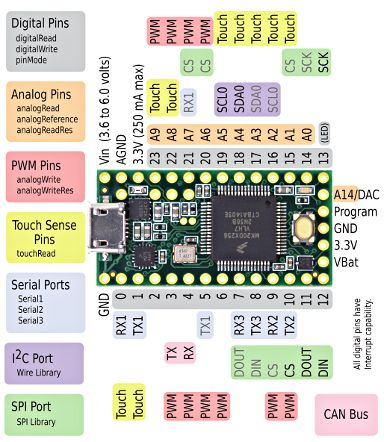
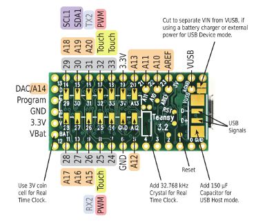
Teensy 3.2 with 256k ram and 32-bit processor $20.00-25.00
Inhaos LCD 2000_7775 $ 4.99
Tactile buttons $ 5.00
Prototype circuit board X 2 ¢ .75
Charger $ .99-4.99
Step up $ .99-4.99
Or powerboost 500 $ 20.00
Micro SD card reader $ 2.50
Wire $ 2.50

As you can see unless you buy the powerboost 500 which is a step up and charger the materials are pretty cheap. I buy in bulk when I can but all prices are for a single piece.

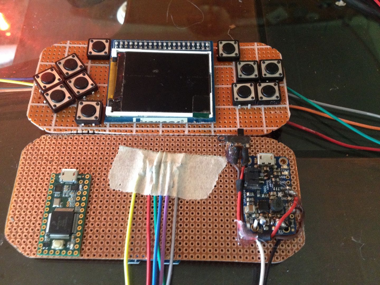
Ok so here's a pic of the system so far. The teensy 3.2 has 10 extra digital io pins so the expansion buttons you see will be ready to use when ever you are ready to program them.

Image

All right so here is the part I need help with.

I'm trying to figure out which pins are actually what on the LCD. As you can see it's missing a couple from the settings file in the GB library. Now the pinouts in the 7775's library define the pin out as

Code: Select all
// pin definition for uno
#define CS     11
#define wr     10
#define rs      12
//#define LE  13

//Plus a whole bunch of data pins that I don't think are needed


But I can see from the schematic there are more that need to be connected to the MCU.

Image

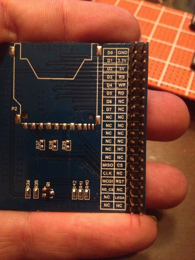
I've got the pins above except for LE, I think it's the Leda pin but not sure.

Here's what I have hooked up to the screen

5v
Ground
Wr
CS
Rs
Rst
Mosi
Clk

I think I need miso too but can't really tell. Also am I right that the SCK pin on the arduino gets 3 different wires? That's what I'm reading from the schematic at least.
User avatar
Duhjoker
 
Posts: 446
Joined: Sat Jul 02, 2016 4:57 am
Location: Where Palm trees grow

Re: Advanced Gamebuino prototype

Postby Duhjoker » Wed Aug 31, 2016 7:58 am

ok so here is the source code for the screen....

.h
Code: Select all
#ifndef LCD_2000_7775_H
#define LCD_2000_7775_H

#if ARDUINO >= 100
 #include "Arduino.h"
 #include "Print.h"
#else
 #include "WProgram.h"
#endif
#include "utility/Adafruit_GFX.h"

#include <avr/pgmspace.h>


#define LCD_2000_7775_TFTWIDTH 176
#define LCD_2000_7775_TFTHEIGHT 220


class LCD_2000_7775 : public Adafruit_GFX
{
   public:
      LCD_2000_7775(uint8_t cs,uint8_t wr ,uint8_t rs , uint8_t rest ,uint8_t pmw );
      LCD_2000_7775(uint8_t cs,uint8_t wr ,uint8_t rs , uint8_t rest );
      LCD_2000_7775(uint8_t cs,uint8_t wr ,uint8_t rs );
      //LCD_2000_7775(){};
      void write_spi(const uint8_t data);
      void drawPixel(int16_t x, int16_t y, uint16_t color);
      void setdatapin(uint8_t b0,uint8_t b1, uint8_t b2 , uint8_t b3,
                                       uint8_t b4, uint8_t b5, uint8_t b6, uint8_t b7);
      void fillRect(int16_t x, int16_t y, int16_t w, int16_t h,
      uint16_t color);
      
      void setbracklight(uint8_t pmw);
      
      void begin();
      
      void drawbitmap(uint16_t* data, uint16_t x ,uint16_t y,uint16_t with , uint16_t height);
      
//fuction
   private:
      void set_window(uint8_t x1,uint8_t y1,uint8_t x2,uint8_t y2);
      void write_wr_reg(uint16_t data);
      void write_wr_data(uint16_t data);
      void write_cmd(uint16_t cmd ,uint16_t data);
      #if 0 //defined(ARDUINO_ARCH_SAM)
         void write_delay();
      #else
         #define write_delay() 
      #endif
      
//value   
   //private:
   
   #if defined(ARDUINO_ARCH_SAM)
      uint32_t _cs;
      uint32_t _pmw;
      uint32_t _wr;
      uint32_t _rs;
      uint32_t _rest;
      
      volatile uint32_t *csport;
      volatile uint32_t *pmwport;
      volatile uint32_t *wrport;
      volatile uint32_t *rsport;
      volatile uint32_t *restport;
      
      uint32_t cspinmask;
      uint32_t pmwpinmask;
      uint32_t wrpinmask;
      uint32_t rspinmask;
      uint32_t restpinmask;
      
      volatile uint32_t data[8];
      volatile uint32_t datapinmask[8];
      volatile uint32_t* dataport[8];   
         
   #else
      uint8_t _cs;
      uint8_t _pmw;
      uint8_t _wr;
      uint8_t _rs;
      uint8_t _rest;
      
      volatile uint8_t *csport;
      volatile uint8_t *pmwport;
      volatile uint8_t *wrport;
      volatile uint8_t *rsport;
      volatile uint8_t *restport;
      
      uint8_t cspinmask;
      uint8_t pmwpinmask;
      uint8_t wrpinmask;
      uint8_t rspinmask;
      uint8_t restpinmask;
      
      volatile uint8_t data[8];
      volatile uint8_t datapinmask[8];
      volatile uint8_t* dataport[8];
   
   #endif
};

uint16_t RGB(uint16_t r,uint16_t g , uint16_t b);

#endif


.cpp

Code: Select all
#include "LCD_2000_7775.h"


LCD_2000_7775::LCD_2000_7775(uint8_t cs,uint8_t wr ,uint8_t rs , uint8_t rest ,uint8_t pmw)
   : Adafruit_GFX(176, 220)
{
   this->_cs = cs;
   //this->_rd = rd;
   this->_wr = wr;
   this->_rs = rs;
   this->_rest = rest;
   this->_pmw = pmw;
   
   pinMode(this->_cs,OUTPUT);
   //pinMode(this->_rd,OUTPUT);
   pinMode(this->_wr,OUTPUT);
   pinMode(this->_rs,OUTPUT);
   pinMode(this->_rest,OUTPUT);
   pinMode(this->_pmw,OUTPUT);
   
   
   this->csport = portOutputRegister(digitalPinToPort(this->_cs));
   //this->pmwport = portOutputRegister(digitalPinToPort(this->_pmw));
   this->wrport = portOutputRegister(digitalPinToPort(this->_wr));
   this->rsport = portOutputRegister(digitalPinToPort(this->_rs));
   this->restport = portOutputRegister(digitalPinToPort(this->_rest));
   
   
   this->cspinmask  = digitalPinToBitMask(this->_cs);
   //this->pmwpinmask  = digitalPinToBitMask(this->_pmw);
   this->wrpinmask  = digitalPinToBitMask(this->_wr);
   this->rspinmask  = digitalPinToBitMask(this->_rs);
   this->restpinmask  = digitalPinToBitMask(this->_rest);
   
   *(this->csport) |= this->cspinmask;
   //*(this->pmwport) |= this->pmwpinmask;
   *(this->wrport) |= this->wrpinmask;
   *(this->rsport) |= this->rspinmask;
   *(this->restport) |= this->restpinmask;      
}

LCD_2000_7775::LCD_2000_7775(uint8_t cs,uint8_t wr ,uint8_t rs , uint8_t rest )
   : Adafruit_GFX(176, 220)
{
   this->_cs = cs;
   //this->_rd = rd;
   this->_wr = wr;
   this->_rs = rs;
   this->_rest = rest;
   
   pinMode(this->_cs,OUTPUT);
   //pinMode(this->_rd,OUTPUT);
   pinMode(this->_wr,OUTPUT);
   pinMode(this->_rs,OUTPUT);
   pinMode(this->_rest,OUTPUT);
   
   
   this->csport = portOutputRegister(digitalPinToPort(this->_cs));
   this->wrport = portOutputRegister(digitalPinToPort(this->_wr));
   this->rsport = portOutputRegister(digitalPinToPort(this->_rs));
   this->restport = portOutputRegister(digitalPinToPort(this->_rest));
      
   this->cspinmask  = digitalPinToBitMask(this->_cs);
   this->wrpinmask  = digitalPinToBitMask(this->_wr);
   this->rspinmask  = digitalPinToBitMask(this->_rs);
   this->restpinmask  = digitalPinToBitMask(this->_rest);
   
   *(this->csport) |= this->cspinmask;
   *(this->wrport) |= this->wrpinmask;
   *(this->rsport) |= this->rspinmask;
   *(this->restport) |= this->restpinmask;      
}

LCD_2000_7775::LCD_2000_7775(uint8_t cs,uint8_t wr ,uint8_t rs)
   : Adafruit_GFX(176, 220)
{
   this->_cs = cs;
   this->_wr = wr;
   this->_rs = rs;
   this->_rest = 0;
   
   pinMode(this->_cs,OUTPUT);
   pinMode(this->_wr,OUTPUT);
   pinMode(this->_rs,OUTPUT);
   
   this->csport = portOutputRegister(digitalPinToPort(this->_cs));
   this->wrport = portOutputRegister(digitalPinToPort(this->_wr));
   this->rsport = portOutputRegister(digitalPinToPort(this->_rs));
      
   this->cspinmask  = digitalPinToBitMask(this->_cs);
   this->wrpinmask  = digitalPinToBitMask(this->_wr);
   this->rspinmask  = digitalPinToBitMask(this->_rs);
   
   *(this->csport) |= this->cspinmask;
   *(this->wrport) |= this->wrpinmask;
   *(this->rsport) |= this->rspinmask;
}


#if 0 //defined(ARDUINO_ARCH_SAM)
   void LCD_2000_7775::write_delay()
   {   
      volatile uint32_t delaycnt = 10;
      while( delaycnt-- );
   }
#endif


void LCD_2000_7775::write_spi(const uint8_t data)
{
   uint8_t bit,i;
   for(bit = 0x01,i = 0 ; bit ; i++,bit <<= 1)   
   {
      if(data & bit) *(this->dataport[i]) |= this->datapinmask[i];
    else   *(this->dataport[i]) &= (~this->datapinmask[i]);
       
    //write_delay();
  }
}

void LCD_2000_7775::setdatapin(uint8_t b0,uint8_t b1, uint8_t b2 , uint8_t b3,
                                       uint8_t b4, uint8_t b5, uint8_t b6, uint8_t b7)
{
   uint8_t i;
   this->data[0] = b0;
   this->data[1] = b1;
   this->data[2] = b2;
   this->data[3] = b3;
   this->data[4] = b4;
   this->data[5] = b5;
   this->data[6] = b6;
   this->data[7] = b7;
   for(i = 0; i < 8 ;i++)
      pinMode(this->data[i],OUTPUT);
   for(i = 0; i < 8 ;i++)
      dataport[i] = portOutputRegister(digitalPinToPort(this->data[i]));
   for(i = 0; i < 8 ;i++)
      datapinmask[i] = digitalPinToBitMask(this->data[i]);
   
   this->setbracklight(255);
}

void LCD_2000_7775::write_wr_reg(uint16_t data)
{
    
    *(this->rsport) &= (~this->rspinmask);
    write_delay();
    *(this->csport) &= (~this->cspinmask);
    write_delay();
    this->write_spi( data >> 8 );
    write_delay();
    *(this->wrport) &= (~this->wrpinmask);
    write_delay();    
   *(this->wrport) |= this->wrpinmask;
    write_delay();
    this->write_spi( (data&0x00ff) );
    write_delay();
    *(this->wrport) &= (~this->wrpinmask);
    write_delay();
   *(this->wrport) |= this->wrpinmask;
   write_delay();
    *(this->csport) |= this->cspinmask;
    write_delay();
}

void LCD_2000_7775::write_wr_data(uint16_t data)
{
   *(this->rsport) |= this->rspinmask;
   write_delay();
   *(this->csport) &= (~this->cspinmask);
   write_delay();
   
   this->write_spi( data >> 8 );
   write_delay();
   *(this->wrport) &= (~this->wrpinmask);
   write_delay();
   *(this->wrport) |= this->wrpinmask;
   write_delay();
   
   this->write_spi( (data&0x00ff) );
   write_delay();
   *(this->wrport) &= (~this->wrpinmask);
   write_delay();
   *(this->wrport) |= this->wrpinmask;
   write_delay();
   
   *(this->csport) |= this->cspinmask;
   write_delay();
}

void LCD_2000_7775::write_cmd(uint16_t cmd ,uint16_t data)
{
   this->write_wr_reg(cmd);
   this->write_wr_data(data);
}

void LCD_2000_7775::set_window(uint8_t x1,uint8_t y1,uint8_t x2,uint8_t y2)
{
   this->write_wr_reg(0x0037);this->write_wr_data(x1); // windows address
   this->write_wr_reg(0x0036);this->write_wr_data(x2);
   this->write_wr_reg(0x0039);this->write_wr_data(y1);   
   this->write_wr_reg(0x0038);this->write_wr_data(y2);   
   this->write_wr_reg(0x0020);  //HS
   this->write_wr_data(x1);       
   this->write_wr_reg(0x0021);  //VS
   this->write_wr_data(y1);
}

void LCD_2000_7775::drawPixel(int16_t x, int16_t y, uint16_t color)
{
   set_window(x,y,x,y);
   //this->write_wr_reg(0x0022);
   //this->write_wr_data(color);
   this->write_cmd(0x22,color);
}

void LCD_2000_7775::fillRect(int16_t x, int16_t y, int16_t w, int16_t h,
      uint16_t color)
{
   set_window(x,y,x+w-1,y+h-1);
   this->write_wr_reg(0x22);
   int i = w*h;
   while(i--)
      this->write_wr_data(color);
}

void LCD_2000_7775::setbracklight(uint8_t pmw)
{
   analogWrite(this->_pmw,pmw);
}

void  LCD_2000_7775::drawbitmap(uint16_t* data, uint16_t x ,uint16_t y,uint16_t with , uint16_t height)
{
   uint32_t i;
   this->set_window(x,y,x+with-1,y+height-1);
   this->write_wr_reg(0x22);
   i = with * height;
   while(i--)
   {
      this->write_wr_data(*data);
      data++;
   }
   
}

void LCD_2000_7775::begin()
{
      if( this->_rest )
      {
             *(this->restport) &= (~this->restpinmask);               
             delay(50); //     Delay 50ms
             *(this->restport) |= this->restpinmask;      
             delay(10); //     Delay 10ms
      }
   
      this->write_cmd(0x0001, 0x011C); // set SS and NL bit
    this->write_cmd(0x0002, 0x0100); // set 1 line inversion
    this->write_cmd(0x0003, 0x1030); // set GRAM write direction and BGR=1,??16BIT 65K?MDT1=0,MDT0=0
    this->write_cmd(0x0008, 0x0808); // set BP and FP
    this->write_cmd(0x000C, 0x0000); // RGB interface setting R0Ch=0x0110 for RGB 18Bit and R0Ch=0111for

    this->write_cmd(0x000F, 0x0e01); // Set frame rate
   
//*************Power On sequence ****************//
    delay(50); //     Delay 50ms
    this->write_cmd(0x0010, 0x0A00); // Set SAP,DSTB,STB
    this->write_cmd(0x0011, 0x1038); // Set APON,PON,AON,VCI1EN,VC
    //delay(50); //     Delay 50ms
    this->write_cmd(0x00ff, 0x0003);    //
    this->write_cmd(0x00b0, 0x1411);    //Set VCOM 1d
    this->write_cmd(0x00b1, 0x0202);    //GVCL/GVDD voltage setting
    this->write_cmd(0x00b2, 0x0313);  //VCL voltage setting

//------------------------ Set GRAM area  set window --------------------------------//
    this->write_cmd (0x0030, 0x0000);//???????
    this->write_cmd (0x0031, 0x00db);
    this->write_cmd (0x0032, 0x0000);
    this->write_cmd (0x0033, 0x0000);//??????
    this->write_cmd (0x0034, 0x00db);
    this->write_cmd (0x0035, 0x0000);//R34H,R35H???????
    this->write_cmd (0x0036, 0x00AF);
    this->write_cmd (0x0037, 0x0000);
    this->write_cmd (0x0038, 0x00DB);
    this->write_cmd (0x0039, 0x0000);
    delay(20);
   
    this->write_cmd(0x00ff, 0x0003);
//    WriteRegister(0x00b0, 0x1d01);
// ----------- Adjust the Gamma Curve ----------//
     this->write_cmd(0x0050, 0x0000);
     this->write_cmd(0x0051, 0x0300);
     this->write_cmd(0x0052, 0x0103);
     this->write_cmd(0x0053, 0x2011);
     this->write_cmd(0x0054, 0x0703);
     this->write_cmd(0x0055, 0x0000);
     this->write_cmd(0x0056, 0x0400);
     this->write_cmd(0x0057, 0x0107);
     this->write_cmd(0x0058, 0x2011);
     this->write_cmd(0x0059, 0x0703);
     delay(50); //     Delay 50ms
     this->write_cmd(0x0020, 0x0000); // Set GRAM Address
     this->write_cmd(0x0021, 0x0000); // Set GRAM Address
     this->write_cmd(0x0007, 0x1017);
   
      
      this->fillRect(0,0,LCD_2000_7775_TFTWIDTH,LCD_2000_7775_TFTHEIGHT,0xffff);
}


/*********************************º¯Êý******************************/
uint16_t RGB(uint16_t r,uint16_t g , uint16_t b)
{
   uint16_t rgb = 0;
   r *= 31;
   r /= 255;
   
   g *= 63;
   g /= 255;
   
   b *= 31;
   b /= 255;
   
   rgb |= (r<<11);
   rgb |= (g<<6);
   rgb |= b;
   return rgb;
}


and here is a example for a graph

Code: Select all
/*
  Arduino LCD-2000-7775 TFT text example For UNO
 
  This example demonstrates how to draw text on the
  TFT with an Arduino. The Arduino reads the value
  of an analog sensor attached to pin A0, and writes
  the value to the LCD screen, updating every
  quarter second.
 
  This example code is in the public domain

  Created 30 April 2014 by INHAOS
 
  http://www.inhaos.com
 
 */


#include <LCD_2000_7775.h>

// pin definition for the Uno
#define cs   11
#define wr   10
#define rs   12
//#define le   13


#define D0    9
#define D1    8
#define D2    7
#define D3    6
#define D4    5
#define D5    4
#define D6    3
#define D7    2


// pin definition for the Leonardo
// #define cs   7
// #define dc   0
// #define rst  1

// create an instance of the library
//LCD_2000_7775 TFTscreen(cs,wr,rs,le);
LCD_2000_7775 TFTscreen(cs,wr,rs);
// char array to print to the screen
char sensorPrintout[4];

void setup() {
 
  // Put this line at the beginning of every sketch that uses the GLCD:
  TFTscreen.setdatapin(D0,D1,D2,D3,D4,D5,D6,D7);
  TFTscreen.begin();

  // clear the screen with a black background
  TFTscreen.background(0, 0, 0);
 
  // write the static text to the screen
  // set the font color to white
  TFTscreen.stroke(255,255,255);
  // set the font size
  TFTscreen.setTextSize(2);
  // write the text to the top left corner of the screen
  TFTscreen.text("Sensor Value :\n ",0,0);
  // ste the font size very large for the loop
  TFTscreen.setTextSize(5);
}

void loop() {

  // Read the value of the sensor on A0
  String sensorVal = String(analogRead(A0));
 
  // convert the reading to a char array
  sensorVal.toCharArray(sensorPrintout, 4);

  // set the font color
  TFTscreen.stroke(255,255,255);
  // print the sensor value
  TFTscreen.text(sensorPrintout, 0, 20);
  // wait for a moment
  delay(250);
  // erase the text you just wrote
  TFTscreen.stroke(0,0,0);
  TFTscreen.text(sensorPrintout, 0, 20);
}


do the buttons need a resistor? the only resistor I see in the schematic looks to be fore the lcd
User avatar
Duhjoker
 
Posts: 446
Joined: Sat Jul 02, 2016 4:57 am
Location: Where Palm trees grow

Re: Advanced Gamebuino prototype

Postby Duhjoker » Thu Sep 01, 2016 1:23 am

Ok so Jonnection had a great explanation of the pin works and General input so I'm gonna place it here..........

jonnection wrote:Hello Duhjoker

DC is data/command select as someone here already pointed out.

What you need to understand, is some basics of the SPI protocol. Its just not a simple question of "what pin does D/C go to?". You need to understand what each pin does. Once you understand what the pins mean, you can start to build any kind of console with any kind of SPI screen.

Image

This is how SPI works:
- there is a master
- there is one or more slaves
- notice, that there are only 4 pins going into each slave

This is what the pins do:
- SCLK is the clock line. Very important. It synchronises the Master and the Slaves to exchange information at the same speed.
- MOSI - Master Out, Slave In. Data from master to slave. This goes from master mosi to slave (lcd) SCR_DIN as you figured out
- MISO - data in the opposite direction
- SS - slave select. In order to tell WHICH slave is supposed to get the next command or data, the Master pulls this pin LOW to talk to each slave. Only one slave should be active at the same time. All other SS lines should be HIGH. SS is often also called CS (cable select) or EN (enable)

Now, you notice now that there is NO DC line in this picture.

How can it be ?

The DC or D/C is a feature, that is specific to the 5110 graphics driver chip. It has nothing to do with the SPI protocol. Therefore, the DC pin can be ANY NORMAL PIN you choose from the Master side. You choose what pin it is, by specifying it in the program code.

So you see, there is no one answer to your question. You need to look at the code and/or copy paste it here to find out what pin on the Master is the DC.
User avatar
Duhjoker
 
Posts: 446
Joined: Sat Jul 02, 2016 4:57 am
Location: Where Palm trees grow

Re: Advanced Gamebuino prototype

Postby Duhjoker » Thu Sep 01, 2016 1:28 am

And summoner123 had this to say......

Summoner123 wrote:Hi DuhJoker.

It will be more simply if we have a Library to interface your display with the Teensy. rsrs

Reading the datasheet at the "Interface Logic Pins" section I have found that:

Image

So the Data/Comand pin is the "RS" pin....


Great work guys I think I might be able to set my LCD up to the teensy 3.2 now!!!

I poured over the over all the info for days and missed that completely. Thank you for the extra eyes!!!!
User avatar
Duhjoker
 
Posts: 446
Joined: Sat Jul 02, 2016 4:57 am
Location: Where Palm trees grow

Re: Advanced Gamebuino prototype

Postby Duhjoker » Thu Sep 01, 2016 1:40 am

I also found these.......

Front of teensy

Image

This is the back.... Look at those inputs!!!!!

Image

Found this too showing where miso and mosi actually are on the board the green parts are for the spi.

Image
User avatar
Duhjoker
 
Posts: 446
Joined: Sat Jul 02, 2016 4:57 am
Location: Where Palm trees grow

Re: Advanced Gamebuino prototype

Postby Duhjoker » Thu Sep 01, 2016 3:42 am

Ok so I think I have the correct pin out for my wiring. It goes like this.....

RS = data command SCR_DC
RST = reset SCR_RST
MOSI = data in SCR_DIN
WR = write enable Needed by the LCD
CS = chip select SCR_CS
RD = read enable Needed by the LCD
CLK= SCR_CLK
5v in
GND

I used the info from the folks above, the GB schematic, the gb .settings file and the pin out offered by the LCD_2000_7775. I'm not seeing any thing about needing a resistor in the LCD info but I could be missing it though I think that's just needed for the Nokia 5110 LCD.

Do I need MISO, I'm not seeing it used for the GB schematic.
User avatar
Duhjoker
 
Posts: 446
Joined: Sat Jul 02, 2016 4:57 am
Location: Where Palm trees grow

Re: Advanced Gamebuino prototype

Postby Duhjoker » Thu Sep 01, 2016 6:33 am

Ok i have a pin out i think will work with the LCD to the teensy. After looking at a ton of pin outs, i learned that the uno and the teensy share the same basic pin out with the teensy having more Digital I/O's.

Mosi to mosi pin 11
RS to A2 pin 16
Rst to A0 pin 14
CS to A1 pin 15
CLK to sck pin 13
WR to pin 10
RD to pin ?

Cant figure out if i need RD its not included in anything i can find.
User avatar
Duhjoker
 
Posts: 446
Joined: Sat Jul 02, 2016 4:57 am
Location: Where Palm trees grow

Re: Advanced Gamebuino prototype

Postby Duhjoker » Thu Sep 01, 2016 6:45 am

I can't figure out why the RS and CS go to different pins on the LCD code example.

Can some one fact check for me I would hate to take a chance at blowing my teensy
User avatar
Duhjoker
 
Posts: 446
Joined: Sat Jul 02, 2016 4:57 am
Location: Where Palm trees grow

Re: Advanced Gamebuino prototype

Postby rodot » Fri Sep 02, 2016 8:15 am

Hello,
You just posted 8 times in a row... please avoid multiple posts if nobody answered, you can edit an existing post if you want to append some new infos.

RD probably doesn't appear in the library because it only supports writing to the screen, not reading from it. So you can probably add a pullup resistor so it doesn't float and leave it as is.

Good luck with your project !
User avatar
rodot
Site Admin
 
Posts: 1290
Joined: Mon Nov 19, 2012 11:54 pm
Location: France

Re: Advanced Gamebuino prototype

Postby Duhjoker » Fri Sep 02, 2016 9:08 am

Sorry about that, I'll make more edits from now on if I need to add something.

My hypothesis with the LCD is that it still needs to use the same basic pins to function and communicate with the teensy the way a Nokia 5110 connects to the uno. Since it uses spi I believe that to be true. But if not please correct me.

Ok so first I wrote down the pin out using the schematic, copying the relevant info from the inside of the uno schematic , pcint0, pc0 etc (I know those don't belong together just an example off the top of my head). After finding a couple more pinouts for the teensy I then took the info from the gb scheme and transposed them over to the teensy. And it's weird I don't feel like I have it right...........

SCR_DC = A2 from the gb code / pc2 = pin 23 A9 teensy
SCR_RST = A0 from the gb code / PC0 = pin 15 A1 teensy
SCR_DIN = 11 from GB code / PB3 = pin mosi A4 or pin 11 //// future question
SCR_CS = A1 from GB code / pc1 = pin 22 A8 teensy
SCR_CLK = 13 from gb code / SCK 13 teensy

But the schematics show two more pins being used besides the power and negative pins. I thought those would be WR and RD but I guess not. Wr actually goes back to SCR_CS which is chip selection on the schematic.

Also according the transposition the mosi goes to A4 but mosi and miso are pins 11 and 12 respectively on the pin out to the teensy. Which should I use.

I noticed a crystal added in the schematics. What is this for?
User avatar
Duhjoker
 
Posts: 446
Joined: Sat Jul 02, 2016 4:57 am
Location: Where Palm trees grow

Next

Return to Hardware Development

Who is online

Users browsing this forum: No registered users and 3 guests

cron